How to make a PCB, part 1: making the schematic for Particle Photon RFM69 board
Many of the projects I plan to cover in the future include designing and building custom PCBs. This is the first post in a series where I’ll be covering how to make a simple PCB, this post in particular covers the process of creating the schematic for the PCB. After this series is complete I’ll begin covering projects like my weather station, and a custom DDS function generator.
PCB design requirements
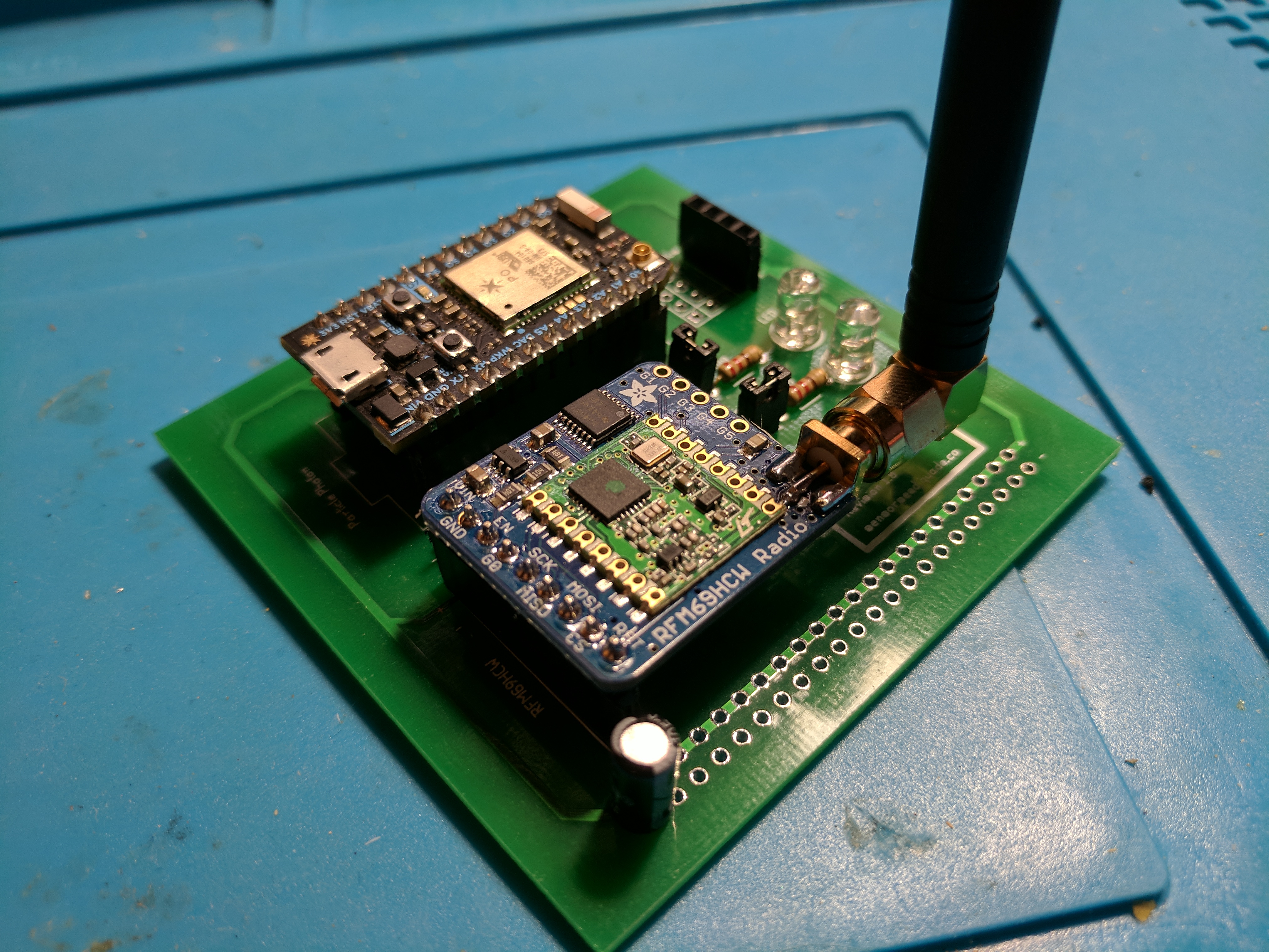
For this series I will be covering the process of making a PCB that connects a Particle Photon to an Adafruit RFM6HCW9 900MHz radio module.This is a very simple board which will give you a good introduction to PCB design. I will be using this same board as the indoor weather data receiver for my weather station project.
Below is a list of requirements I would like to meet with my design.
- Headers that can connect to a Particle Photon.
- Headers that can connect to the Adafruit RFM69HCW module.
- Power LED, along with a pin controlled LED.
- Ability to physically disable the LEDs using jumpers.
- Use of entirely through hole components.
- An I2C bus for possible future upgrades.
- Power input pins.
- An extra power rail for possible future upgrades.
- Small board size to keep production costs low (under 10x10cm).
In general the board should be small, connect the Particle Photon to the RFM69HCW radio, and be flexible enough to handle future upgrades. An example of an upgrade would be adding an I2C based indoor temperature sensor.
Schematic and PCB layout (EDA) software options
There are many programs that you can use for your schematics and PCB layouts. You can find a list of EDA software on Wikipedia. Popular programs include KiCad, Eagle, and gEDA.
Eagle seems to be the most popular EDA program at the time this post was written. The problem with Eagle is it costs a lot of money, and they have moved over to a subscription based license which costs even more in the long run. For that reason a lot of people are switching over to KiCad which has been increasing in popularity a lot.
I’ll be using gEDA for my schematic and board layout for this project. gEDA isn’t the most popular EDA, but it is stable, simple, and completely free and open source. It is also what I am the most familiar with since I have been using it at work.
gEDA is a collection of EDA programs. For schematics you can use a program called gschem, and for PCB layout you can use a program called pcb. There is also a gerber file viewer which is useful when reviewing your PCB layout before sending it off to be manufactured.
You can download gEDA as a software package in many Linux distributions. There is also a Windows version, but I haven’t used it. I personally use the Linux version through X11 forwarding from the Bash for Windows Ubuntu subsystem.
gEDA schematic program overview
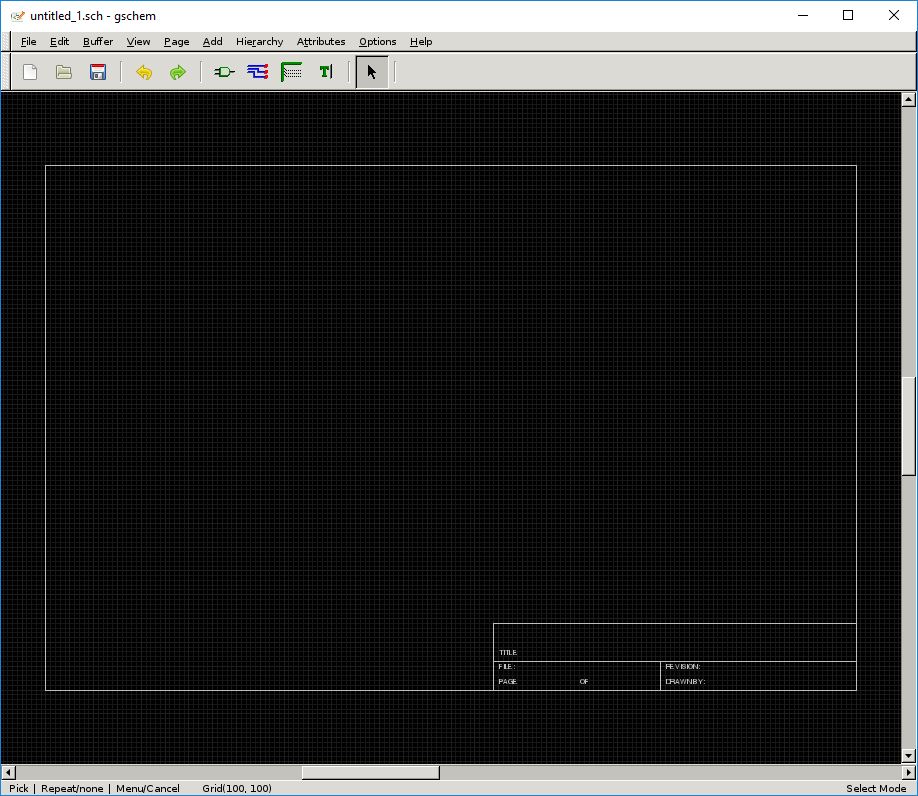
To get started with gschem simply open the program by typing the following into your console.
gschem
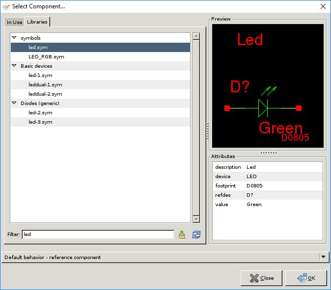
As an example we can wire an LED to a power supply through a resistor. gEDA has a lot of shortcut keys used to access various menus. To add components type in “ac” without quotes. A new dialog box will appear where you can search for components.
Search for LED, and find one you like. Click ok, and place the component by clicking, and press the escape key to leave the place mode. You can then repeat the process to place a resistor, along with VCC and GND points.
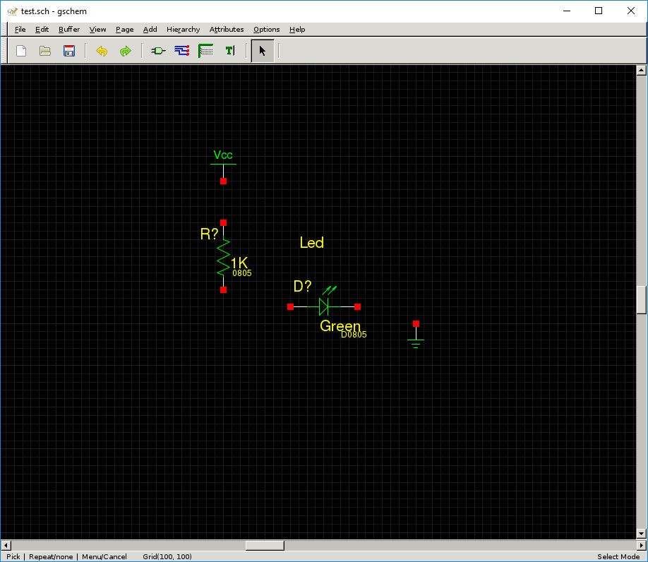
With all of the components placed you’ll want to arrange and connect them. A useful key combination is “er” which rotates the component. Components are connected using nets, hover over one of the red edges of a component and type “an” to add a new net, then click on the red box you want to connect the other end of the net to. Press the escape key to leave the add net mode. Repeat the process until all of your components are connected.
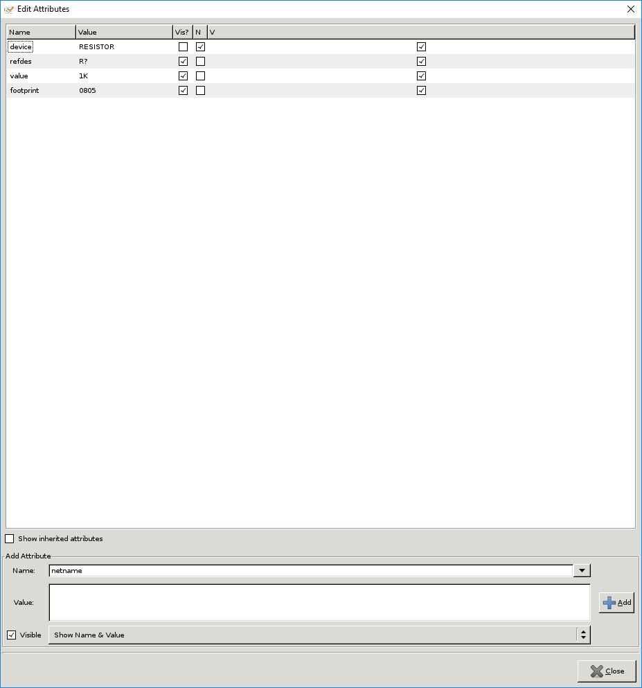
You might have noticed that the components have default values, like 1K for the resistor. To change these values click on the component and type in “ee”. A new window will appear with a list of properties. In the case of a resistor give it a unique number for refdes, like R1, and give it an appropriate value, like 220. You can ignore other properties like footprint until we start on the PCB layout. Double click on the value boxes to set the value.
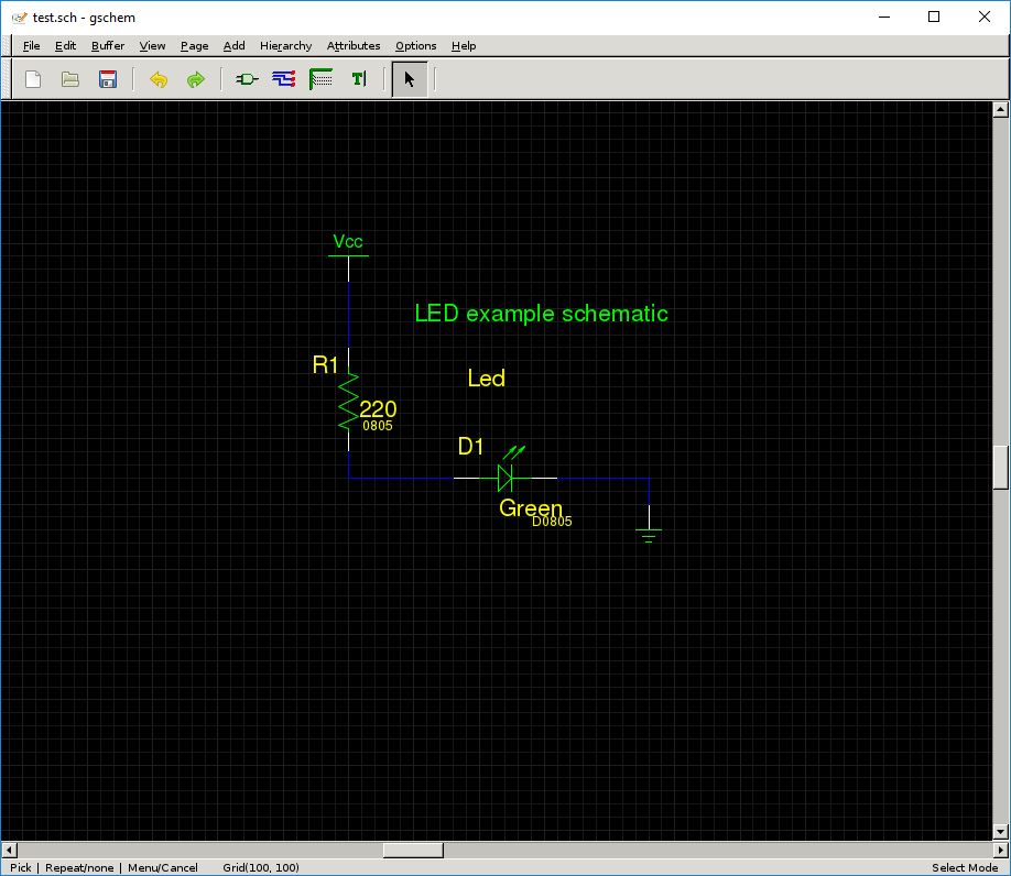
Another useful key combination is “at” which allows you to add text to the schematic as a label.
gEDA schematic symbols overview
Searching for components in gschem reveals that there is a very limited selection of parts, or symbols. To add the parts you want to use you’ll need to either find them online from places like GedaSymbols, or make them yourself using this guide.
Add the following line to a file located at “~/.gEDA/gafrc” to tell gEDA where your symbols are installed. Restart gschem for the new symbols to show up in the component list.
(component-library “/home/user/.gEDA/symbols”)
I have created a GitHub repository that includes all of the symbols and footprints I have used while making this series of posts. You can clone the repository and copy the footprints and symbols into your gEDA folder. Please leave a comment if I forgot to add a file and I’ll add it to the repository.
I also included the LED example schematic, and the Particle Photon board schematic to that same repository.
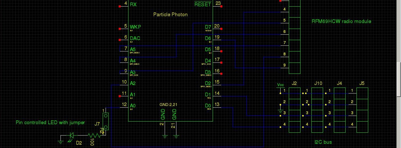
Particle Photon RFM69 board schematic
Now you should have a pretty good understanding of how to use the gschem program within gEDA to create schematics. Creating more complicated schematics, like the Particle Photon RFM69 board, is just like creating the simple LED circuit, but with more components.
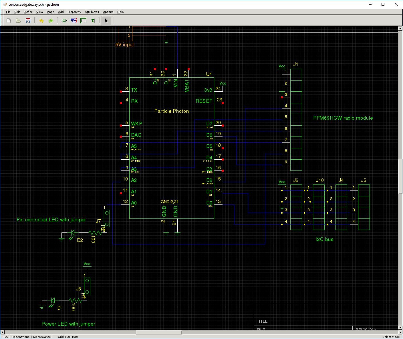
Above is an image showing the schematic of the Particle Photon RFM69 board. At the center is a Particle Photon. Going around the board starting at the top left you can see the following pieces.
- 3.6-5.5V power input connector, connected to the VIN on the Particle Photon.
- RFM69HCW radio module connected to the power rail, along with SPI and other pins on the Particle Photon.
- Four sets of I2C inputs connected to the I2C pins on the Particle Photon, and the power rail.
- The power LED connected directly to the power rail through a jumper, and a resistor.
- The controllable LED connected to the A0 pin on the Particle Photon through a jumper, and a resistor.
Conclusion
Creating a schematic using gEDA is a straightforward process. I find the only tricky part being the process of finding all of the component symbols and footprints I’m looking for. Other than that part it isn’t too different from drawing a schematic on a piece of paper which you are probably already familiar with.
I’m planning to create a few more posts in this series on how to make a PCB. Here’s a list of those planned posts.
- Making a schematic (this post)
- Making a schematic symbol
- Creating a PCB footprint
- Making a PCB layout
- Manufacturing the PCB
I don’t have any specific schedule for these posts, and the order isn’t set in stone. I may end up writing the posts on creating schematic symbols and PCB footprints after all of the others since they aren’t quite as important if you can find the symbols and footprints online.
William – would you be willing to post the Gerber file and/or particle code for this project? I’m trying to create a Photon RFM69 gateway too and I’m mulling over whether I should try to create something like this or use a gen 3 particle device with an RFM69 feather board. Thanks!