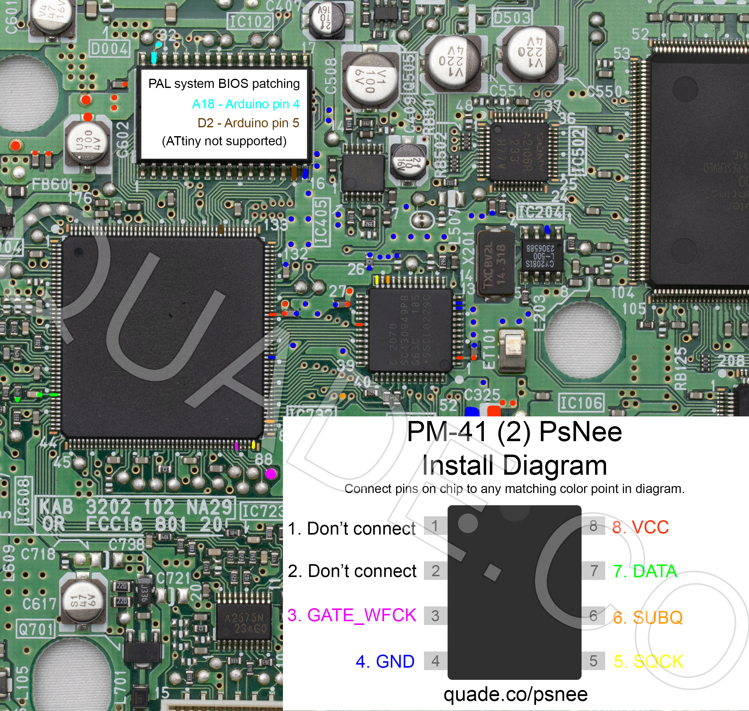
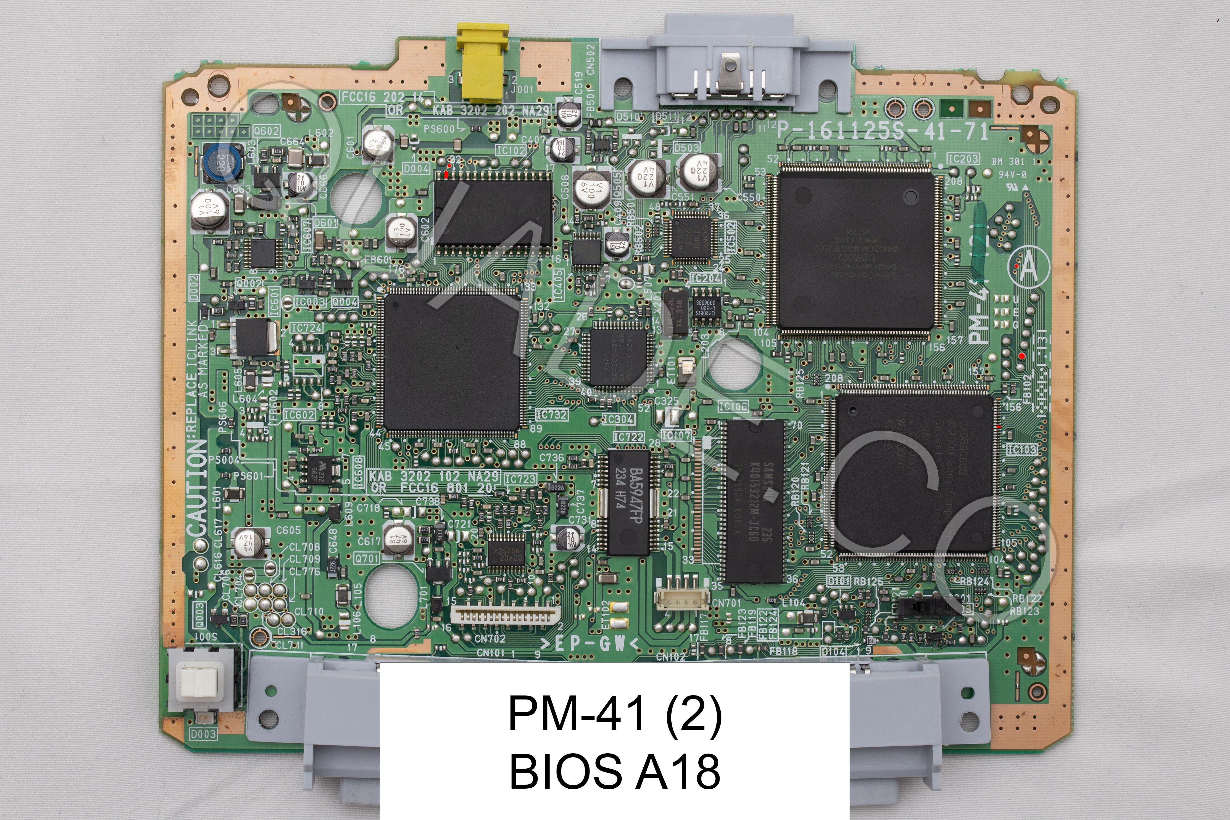
PM-41 (2) PsNee modchip installation diagram
Towards the end of the SCPH-10x PSone production Sony revised the board slightly and released the PM-41 (2) board. This page covers the installation diagram for installing a PsNee chip into the PM-41 (2).
If your board has PM-41 printed on it then you should follow the PM-41 guide instead.
For more information about PsNee chips click here, for more information about PS1 modchips click here.
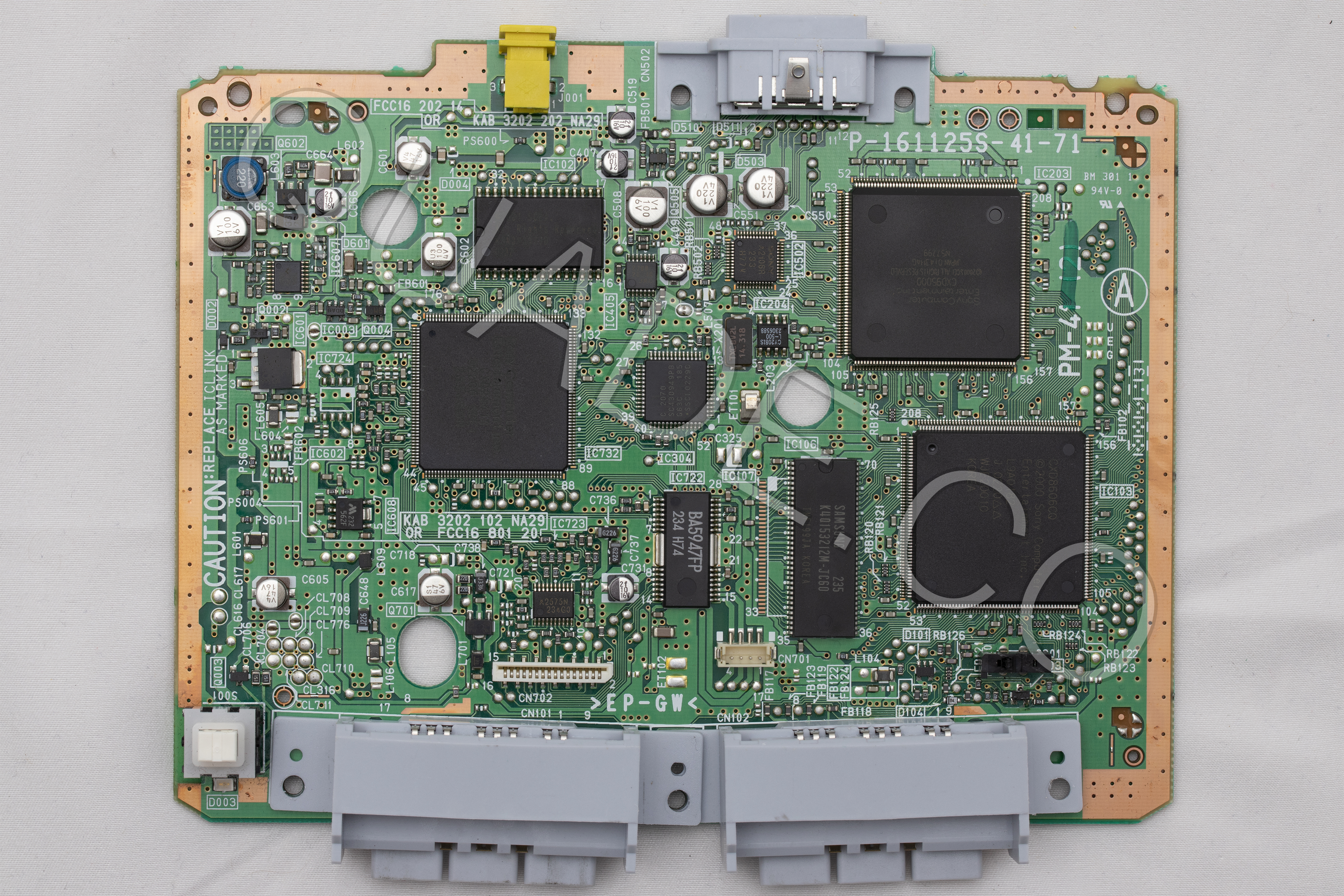
PM-41 (2) board components and fuse locations
Here are a couple of photos of the PM-41 (2) board. If you click on them they’ll open in a much higher resolution format so you can zoom in on the details. This first image shows the front of the board (marked with the letter A).
This second image shows the back of the board (marked with the letter B).

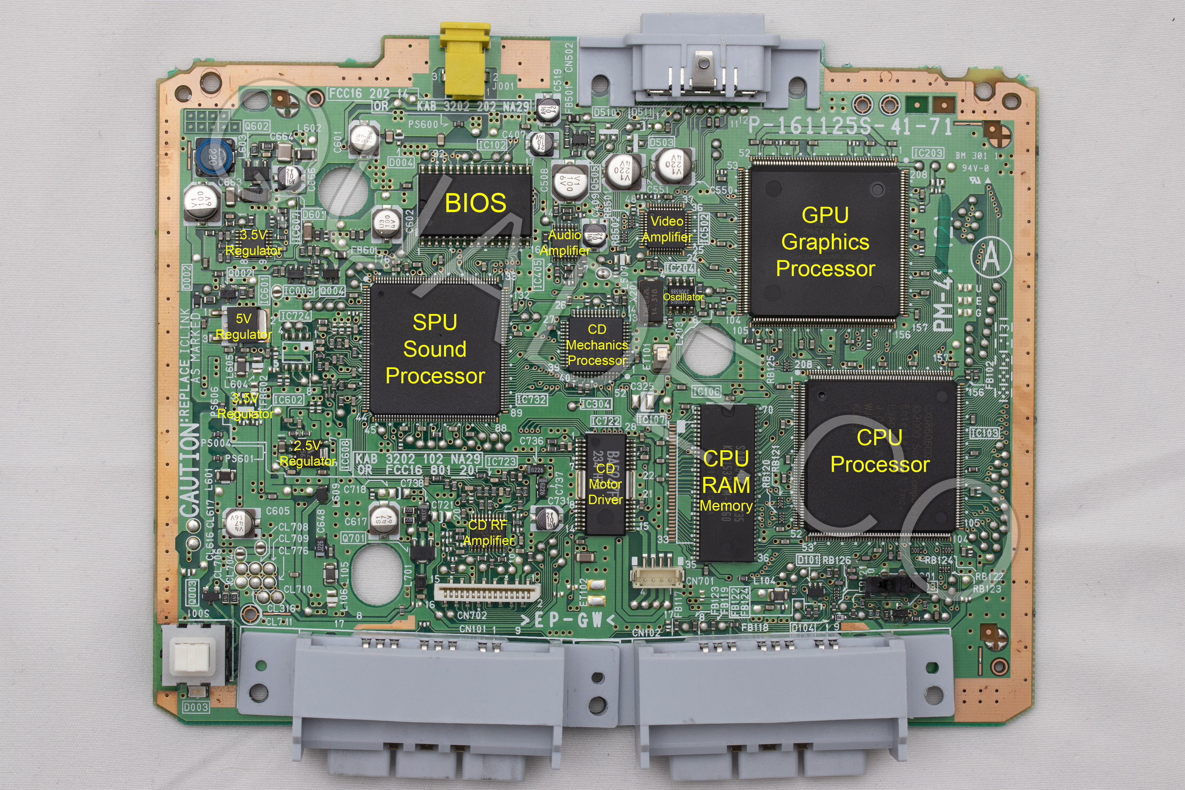
Below is that picture of the front of the board again, but this time it has labels on all of the major board components. This can be useful if you are debugging an issue on the system. For example if your video output is bad you might want to try replacing the capacitors near the video amplifier.
Another common issue people run into is blown fuses. Below is a diagram showing the locations of all of the fuses on the PM-41 (2) board. They are highlighted in yellow, with the fuse value nearby.

PM-41 (2) PsNee modchip installation diagram
Arduino pinout:
- Pin VCC – VCC
- Pin GND – GND
- Pin 3 – Debug TX
- Pin 4 – BIOS A18
- Pin 5 – BIOS D2
- Pin 6 – SQCK
- Pin 7 – SUBQ
- Pin 8 – DATA
- Pin 9 – GATE_WFCK
Above is the installation diagram. Just match each colored pin label in the diagram with any matching colored point on the board. Click on the image for a higher resolution version. I recommend placing the modchip on top of the CD mechanics processor chip.
If you have a PAL PSone system then you’ll need to use an Arduino board and connect A18 and D2. Otherwise just ignore A18 and D2.
I have created additional diagrams primarily for colorblind people. They show one point at a time in a single color (there is a set in red, green, and blue). Because they show the entire board they may reveal more alternative points for each pin. Click on the links below to reveal the sets of images.
I’m creating these new diagrams for each PS1 board revision working from newest revision to oldest revision. It’s going to take some time, but should hopefully be more helpful than the older diagrams I had on here before.
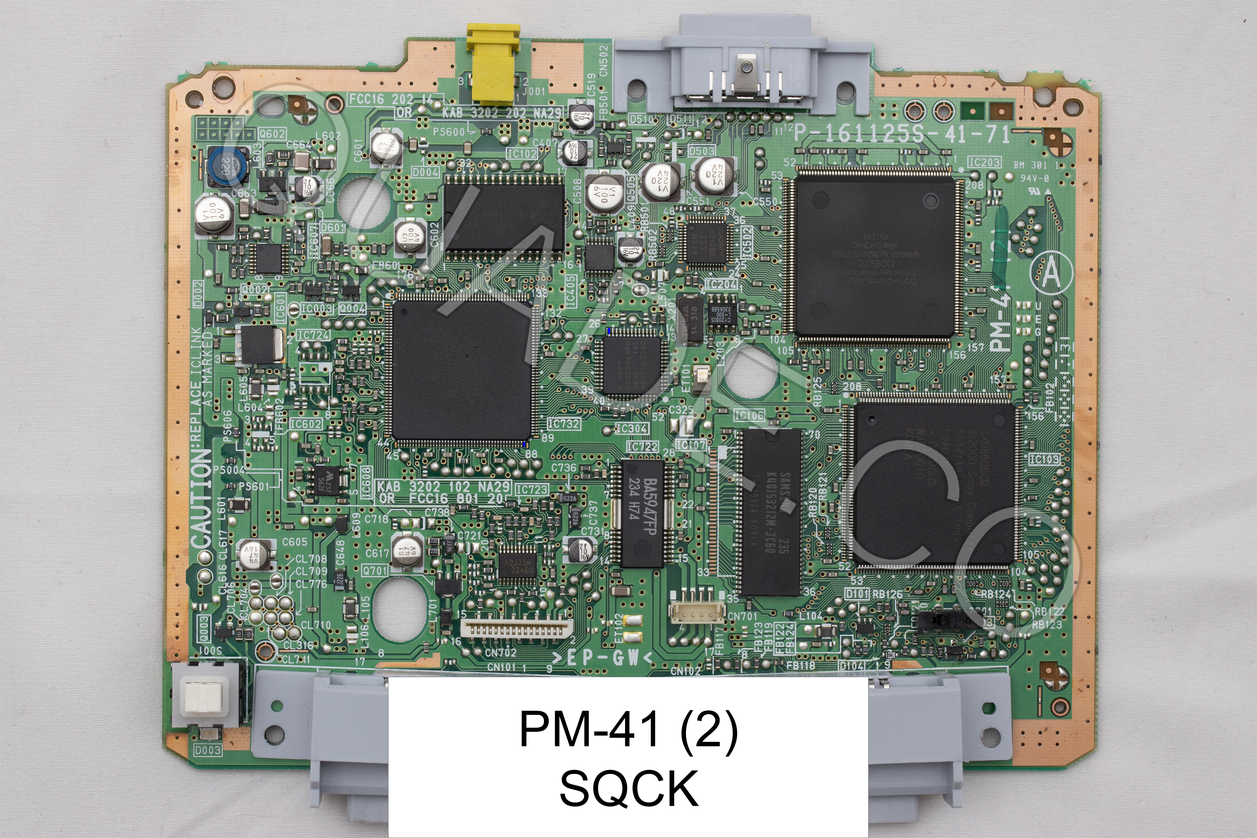
PM-41 (2) PsNee modchip installation diagram (one diagram per pin, colored in red)
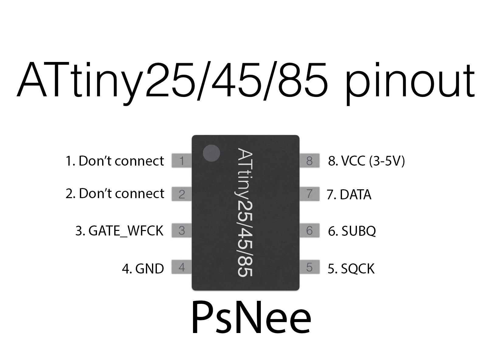
Click on the images to see them in higher resolution. Pin numbers are for the ATtiny.
GATE_WFCK: Pin 3

GND: Pin 4

SQCK: Pin 5

SUBQ: Pin 6

DATA: Pin 7

VCC: Pin 8

BIOS A18 (not for ATtiny)
BIOS D2 (not for ATtiny)

PM-41 (2) PsNee modchip installation diagram (one diagram per pin, colored in green)
Click on the images to see them in higher resolution. Pin numbers are for the ATtiny.
GATE_WFCK: Pin 3

GND: Pin 4

SQCK: Pin 5

SUBQ: Pin 6

DATA: Pin 7

VCC: Pin 8

BIOS A18 (not for ATtiny)

BIOS D2 (not for ATtiny)

PM-41 (2) PsNee modchip installation diagram (one diagram per pin, colored in blue)
Click on the images to see them in higher resolution. Pin numbers are for the ATtiny.
GATE_WFCK: Pin 3

GND: Pin 4

SQCK: Pin 5
SUBQ: Pin 6

DATA: Pin 7

VCC: Pin 8

BIOS A18 (not for ATtiny)

BIOS D2 (not for ATtiny)

Installation tips
Here are some tips I have for you when you are soldering your chip into the PM-41 (2).
- Cut your wires to be as short and direct as possible.
- You don’t need to connect pins one and two of the ATtinyX5 chip. Just desolder the wire.
- If you are using an ATtinyX5, or have a SCPH-101, then ignore pins A18 and D2.
- Use a multimeter to probe around for alternative VCC and GND points closer to where you position your chip for a cleaner installation.
- There may also be easier to solder to points for SQCT and SUBQ.
- Be super careful when soldering SQCT and SUBQ. It’s easy to bridge pins if you aren’t careful.
- Be careful with the DATA connection, it’s easy to accidentally knock the capacitor off the board.
Example installations
This section has photos of some successful installations which you can use to get a better understanding of how everything is wired and positioned.
Here are some sample installations I have done in SCPH-101’s:
- Nobody yet.
I am no expert but was able to install properly on the first try! Having options for most of the connection points makes it much less intimidating, good luck to anyone else doing this mod
Hi. Do you have a diagram with photo for an installation with arduino? Thanks! I’m looking for this PM 41(2) NTSC model but I can’t find anyone…
Just match the Arduino pinout list (above the diagram) with the ATtiny diagram. For example SQCK is pin 6 on the Arduino, and pin 5 on the ATtiny diagram. Debug TX, BIOS A18, and BIOS D2 aren’t necessary unless you have a PAL system.
Thanks! I will do that. Also… how do I know the region of my PSOne? I have some serious doubt if its truly NTSC. It says in the mobo SC430949PB. Thanks again.
The easiest way to find out would be to try booting a retail NTSC game without a chip installed. If it boots then it’s an NTSC console, if it doesn’t then it’s a PAL console. I don’t think the boards have any obvious region identifying info printed on them.
Thanks for you answer! I will do that. Also… I have a doubt about if my PSOne is truly NTSC. My mobo (PM41[2]) says SC430949PB.
Hey, today i manage to program and install a Psnee, and successfully install on a pm-41 (2). To program i used an Arduino Uno and a breadboard, and an Attiny85. Here’s a photo of it installed, it’s covered in eletrical tape because i wasn’t sure it was going to touch the metal shielding from de psone. https://imgur.com/a/SnK15EC PS: Quade, most of the tutorials i’ve seen on youtube and your guides here, don’t touch on the subject of “burning the fuses” on ArduinoIDE, using the “burn bootloader” option. Since im new to arduinos and programing chips, i was unaware this step… Read more »
Just installed my first mod chip thanks to this guide and your chip. Me and the roommate have already been exploiting it, and it works great!
hello i did uncomment both arduino board and region check and installed a pro mini too with all the wiring including pins 4 and 5 while it runs pal backups very good it cant run ntsc ones my console is ntsc
Reporting success with an ATtiny85 and a US NTSC PM-41 (2) mobo.
Worked first try. Nice diagram!
In the diagram, the pin for GATE_WFCK is connected to a wrong pin of that big IC (pin 76 instead of pin 84), see https://www.obscuregamers.com/threads/psone-pm-41-2-a-modchip-problem.618/page-2#post-3859