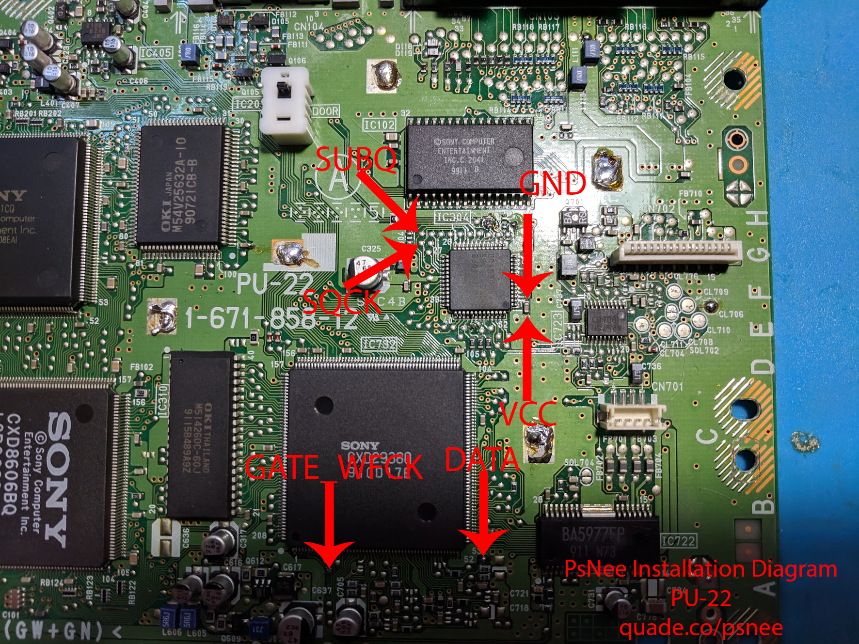
PU-22 PsNee modchip installation diagram
This is my favorite version of the PlayStation 1. It’s in newer systems, so the lasers are more likely to still be in good condition, but the system still has both the serial and parallel ports on the back. This board was used primarily with the SCPH-7500 series of systems.
For more information about PsNee chips click here, for more information about PS1 modchips click here.
PU-22 PsNee modchip installation diagram
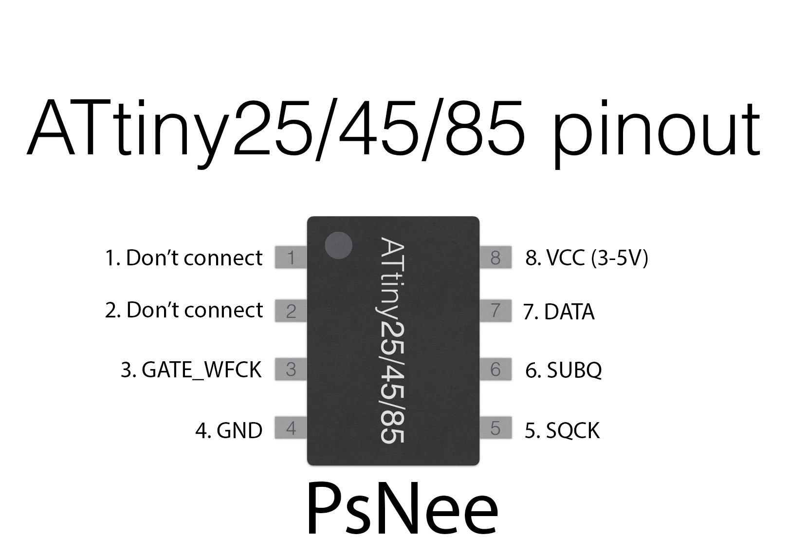
Arduino pinout:
- Pin VCC – VCC
- Pin GND – GND
- Pin 3 – Debug TX
- Pin 4 – BIOS A18
- Pin 5 – BIOS D2
- Pin 6 – SQCK
- Pin 7 – SUBQ
- Pin 8 – DATA
- Pin 9 – GATE_WFCK

Above is the diagram for the PU-22.
This diagram is fairly straightforward. Be careful when soldering to the capacitor that connects to VCC and GND. In particular, the GND point can easily be bridged to nearby pins/pads.
Installation tips
Here are some tips I have for you when you are soldering your chip into the PU-22.
- Cut your wires to be as short and direct as possible.
- You don’t need to connect pins one and two of the ATtinyX5 chip. Just desolder the wire.
- Use a multimeter to probe around for alternative VCC and GND points closer to where you position your chip for a cleaner installation.
- Placing the chip on top of the chip in between SUBQ, SQCK, GND, and VCC is a good spot.
- Watch out for solder splatter when you are desoldering the metal shield on top of the board. It isn’t necessary to put it back on, but I always do.
Example installations
This section has photos of some successful installations which you can use to get a better understanding of how everything is wired and positioned.
- Jon Co

Success! I messed up my first attempt by not keeping the leads extremely short. I’m sure it bridged a few traces. It wouldn’t boot backups without glitches. I went back and took my time making sure each connection was right and now it works flawlessly.
Any better locations to pull power from besides the SMD capacitor? My soldering iron has no temperature control and I keep making it come off
You can use pin 1 from my MM3 diagrams for VCC and pin 8 from my MM3 diagrams for GND.
I don’t have a vcc called pin on my Arduino nano is there a different name for it?
You can try using the VIN pin. The Nano is only officially compatible with 5V but it may work at 3.5V (what the diagram’s VCC point voltage is).
I just installed this based on the instructions. Looks like the Vcc/Gnd has the polarities reversed in your diagram.
Yeah, looks like you’re right. I updated the diagram.
I tore off the GATE_WFCK pad. Is there anywhere else I can connect the wire?
If you follow the little trace line that connects to the pad you’ll see that it connects to one of the pins on the chip above it. Be careful though, it can be tricky to solder to the pin without bridging solder across multiple pins.
I know the trace connects to a nearby pin, but I didn’t attempt soldering a wire to it because the pitch is so fine I’d probably ruin it with bridging
That’s the only other location for that pin, so you’ll likely just need to get your hands on a replacement board.
This happened to me as well, so I soldered directly to the pin with flux by having as few solder as possible on the tip and soldering a single strand from a multistrand copper wire
Tricky, but that worked
That happened to me too. For info in case anyone is in the same situation, instead of soldering directly onto the chip pin (which is rather tricky) I ended up scratching away the protective material from the thin track leading to the pad, raising it from the board and soldering the wire to it (and taping it down just to avoid further damage). It is tricky but still a lot easier than soldering directly onto the leg and helps avoid any bridges.
Here’s my contribution, using a Attiny85. The only difference being that i took ground from other pad.
https://imgur.com/a/cZyAMPS
Okay, I just did some testing with the Attiny85 and it does not play nicely with something like Tony Hawk Pro Skater 2, and it did not boot the backup. I will have to order some 45s or use the Mayumis I ordered from you.
ATtiny85 chips should work if programmed properly. They’re identical to the 25/45 except for the amount of memory they have.
It works with Konami games, legit SRWF, Fatal Fury, but curiously NOT Tony Hawk Pro Skater 2 on like the second boot or something. I have read that the 85 has limitations compared to the 45, and I guess I found one.
I accidentally pulled off the DATA pad. Is there an alternative one?
You’d have to follow the trace up to the large chip to the top left of the DATA pad. One of the small pins on that chip connects to the DATA pad. It can be tricky to solder to it though.
Thanks. I thought there might be one there!
can i use this diagram for the connections of PsNee on a arduino mini pro?
Yes, but the pin numbers will be different. On the post I list the Arduino pin numbering.
what are the pin outs for an Arduino uno r3
See the Arduino pin out list in the post.
I accidentally lifted the capacitor for the VCC and GND wires. Do you know if that capacitor is polarized?
No, it’s not. Can go back on in any orientation.
thanks so much for this guide! i’m new to soldering and the guide was simple enough for me to follow correctly 🙂
I somehow lost the pcb substrate solder pad for the subq connection. Can I just hardwire some wire from the through hole that the circuit appears to go through, directly to the top pin on the IC304, 3rd from the left? It looks like the circuit goes all the way through? I am not sure the exact function of subq, though so I am not sure if that is possible. Is there a better way at getting around this?
Yes, you can use a wire to replace the part of the trace/pad you lifted off. It’s necessary to replace it otherwise the system won’t read games.
It is done. I have finally installed the chip and it works great. Thank you for your help.